An In-Depth Look at GaN Technology and Its Role in GaN Chargers

In the fast-paced world of power electronics, advancements and innovations play a crucial role in shaping the industry. One such breakthrough technology that has been making waves is Gallium Nitride (GaN) technology. With its incredible potential to revolutionize power electronics, GaN technology has emerged as a game-changer. We’ll uncover the innovative features and capabilities of GaN (Gallium Nitride) and its transformative impact on the development of chargers. From the enhanced energy-saving and compact design to the accelerated charging speeds, GaN technology is redefining the landscape of charging solutions.
What is Gallium Nitride?
Gallium nitride (GaN) is a very hard, mechanically stable, binary III/V direct bandgap semiconductor. With higher breakdown strength, faster switching speed, higher thermal conductivity and lower on-resistance, power devices based on GaN significantly outperform silicon-based devices.
Gallium nitride (GaN) is a semiconductor material with unique properties, very hard texture, and a wurtzite crystal structure. GaN was first commonly used in blue light-emitting diodes in the 1990s, and its application range has continued to expand since then. It has been used in solar panels to convert light into electricity, and now it has made significant progress in the field of transistors, gradually replacing silicon as the preferred semiconductor material.

GaN charging technology presents a host of benefits that position it as a compelling alternative to conventional silicon-based chargers. GaN possesses nearly triple the bandgap of silicon, enabling larger breakdown voltages and greater thermal stability at higher temperatures. Its breakdown field significantly surpasses silicon, making GaN more adept at supporting high-voltage designs.
Additionally, GaN’s superior electron mobility allows for higher switching frequencies, presenting several distinct advantages over silicon in semiconductor applications. Also, it is widely used in power electronics components such as resistors, capacitors, inductors, transistors (MOSFETs and IGBTs), thyristors, and diodes. These components play a crucial role in controlling electricity flow, storing energy, and switching electric currents in power electronics systems.
Compared to other semiconductor materials like Silicon (Si) and silicon carbide sic, GaN offers higher conductivity due to the high mobility of electrons within its crystal structure. GaN has a wider bandgap of 3.4 eV, while SiC has a bandgap of 3.26 eV and Si has a bandgap of 1.12 eV. This wider bandgap gives gan power technology several advantages, including higher power density, operation at higher voltages and temperatures, reduced switching losses, and lower manufacturing costs.
The prospects for GaN technology are promising, driven by the increasing demand for power electronics solutions with low power consumption and improved energy efficiency. The market for GaN semiconductor devices is projected to grow at a compound annual growth rate of 24.4% from 2022 to 2030, reaching a value of USD 12.47 billion by 2030.
GaN technology finds application in various industries and segments that rely on power electronics. It is commonly used in RF power transistors, FETs, IGBTs, and power ICs. GaN enables the development of wireless telecommunication modules with enhanced functionalities, supporting applications such as 5G wireless communication, base stations, terminals, and point-to-point data transmission.
The use of GaN material contributes to lower energy consumption and longer device operation, making it suitable for industries such as automotive (electric vehicles), consumer electronics, healthcare, industrial, and communication technology.
GaN technology offers advantages in power electronics, driving its adoption and growth in various industries. Its wider bandgap, high conductivity, and cost-effectiveness make it a preferred choice for creating advanced power electronics solutions.
Physical Properties of Gallium Nitride:
Gallium nitride (GaN) possesses unique properties as a material. It consists of gallium, which has an atomic number of 31, and nitrogen, which has an atomic number of 7. These two elements combine to form a robust Wurtzite structure, which imparts strength to the material and gives it a high melting point of approximately 2500°C.
Unlike naturally occurring substances, GaN is not found in nature and must be synthesized chemically. The synthesis process involves subjecting gallium and ammonia to high temperatures and pressure.
However, there are challenges associated with GaN due to limitations in achieving desired size and purity. It has a complex crystal structure referred to as the Wurtzite structure, which can result in high dislocation densities ranging from 1 in 10^8 to 1 in 10^10 defects. These dislocations can impact the material’s performance and characteristics.
| Main Physical Properties Of Gallium Nitride | ||
|---|---|---|
| PROPERTIES | UNITS | SILICON CARBIDE |
| Density | g/cm3 | 6.1 |
| Hardness | GPa | approx 12 |
| Fracture Toughness | MPa.m1/2 | Approx 0.80 |
| Thermal Expansion Coefficient | 10-6/°K | / |
| Thermal conductivity | W cm-1 °K-1> | 1.3 |
| Refractive index | Not applicable – ratio only | 2.429 |
| Solubility | Not applicable | Insoluble |
| Melting point | °C | ~2500 |
Electrical Properties of Gallium Nitride:
Gallium nitride (GaN) is a semiconductor with unique electrical properties that make it highly useful in various devices such as GaN Schottky diodes, GaN FETs, GaN MOSFETs, and GaN HEMTs.
GaN is classified as a wide bandgap semiconductor due to its hexagonal crystal structure. It has a bandgap energy of 3.4 eV, which is over three times that of silicon. This wide bandgap property allows GaN to operate at higher temperatures and sustain higher voltages, making it ideal for use in semiconductor devices like GaN FETs, GaN MOSFETs, and GaN HEMTs.
The bandgap of a semiconductor determines its ability to conduct electricity, and GaN’s wide bandgap enables it to offer higher coherence and resilience in power applications, including power supplies and RF power amplifiers.
| PROPERTY | SI | GAN |
|---|---|---|
| Energy Band Gap: EG(eV) | 1.12 | 3.2 |
| Electron Mobility: µn(cm2/VS) | 1400 | 1250 |
| Breakdown Field: EB(V/cm)X106 | 0.3 | 3 |
| Saturation Drift Velocity: vs(cm/s)X107 | 1 | 2.7 |
| Relative Dielectric Constant: eS | 11.8 | 9.5 |
Also, the advent of GaN in transistors signifies a significant breakthrough in the electronics industry. Its exceptional characteristics, such as high electron mobility and superior thermal conductivity, make it an ideal candidate for high-performance electronic devices. GaN transistors offer higher power density, and enhanced switching speeds compared to their silicon counterparts.
The reduced heat generation in GaN chargers allows for a more compact design without compromising power output or safety. By bringing components closer together, APPHONE GAN chargers are able to achieve smaller form factors while maintaining high performance and ensuring safety standards are met.
Benefits of GaN Technology:
- Lightweight Build: GaN’s high switching frequency enables smaller inductors and capacitors, reducing the weight and volume of devices, contrary to the misconception that small devices are always lightweight due to their size.
- Cost Efficiency: Despite higher initial costs, GaN transistors ultimately reduce overall system costs by downsizing the device’s components.
- Enhanced Energy Efficiency: GaN technology maximizes energy efficiency by sustaining higher temperatures, ultimately reducing energy consumption and enhancing device effectiveness for chargers, LEDs, and other tech.
- Accelerated Processing Speeds: Utilizing smaller working parts and higher switching frequencies, GaN technology enhances processing power and energy-saving.
- Improved Durability: Mechanically stable with higher breakdown strength, devices using GaN technology withstand demanding operating conditions and are less prone to failures.
- Higher Power Density: GaN’s high thermal conductivity and low on-resistance result in increased power density, delivering more power in a smaller package.
- Versatility: Versatile GaN technology finds application in LED lighting, power supplies, rapid chargers, and automotive settings, offering an attractive option for enhancing product performance.
Gallium Nitride Applications:
GAN technology charger have diverse applications across various industries, offering advantages such as fast charging, high power output, and compact design.
- Mobile Devices and Smartphones: GaN chargers are ideal for charging smartphones and mobile devices quickly. They provide fast power-ups, ensuring convenient usage for users who heavily rely on their devices.
- Laptops and Ultrabooks: GaN chargers are well-suited for powering laptops and ultrabooks, delivering higher power levels to enable faster charging. Their compact design is particularly advantageous for professionals who frequently travel with their devices and require good charging solutions.
- Electric Vehicles (EVs): GaN chargers play a significant role in electric vehicle charging. With their high power output, GaN-based chargers contribute to faster charging times for EVs. This capability supports the broader adoption of electric transportation by providing convenient and better charging solutions.
Industrial and Medical Devices: GaN chargers find applications in the industrial and medical sectors where high power requirements and compact form factors are crucial. They charge a range of devices, including industrial sensors, medical equipment, and portable devices used in healthcare settings. gan technology charger offer the advantage of reliable and rapid charging for critical devices in these industries.
Enhance Your Charging Experience with GaN Charging Technology.
As the demand for ultra-fast power supply and charging continues to grow, GaN (gallium nitride) is emerging as a promising alternative and a future replacement for silicon.
GaN technology has revolutionized the field of chargers by significantly reducing heat generation compared to traditional silicon-based devices. This is due to GaN’s faster and more coherent operation, which minimizes the workload on components. With GaN technology, bulky chargers, slow charging times, and safety concerns are becoming a thing of the past. GaN chargers offer a compact design, high efficiency, and powerful performance, making them perfectly suited for the demands of our modern lifestyle.
At APPHONE, we offer a wide range of GaN chargers. Whether you need a charger for the latest devices or one with multiple ports to cater to all your charging needs, we have you covered. With APPHONE, it’s not just about connecting your power – it’s about seamlessly connecting every aspect of your life.
Future Trends and Challenges in GaN Technology:
The future of gan charger technology presents several trends and challenges that will shape its widespread adoption and application.
- Integration of GaN Technology in Infrastructure: Gan charging technology has the potential to revolutionize charging infrastructure, enabling faster charging in public spaces, homes, and workplaces. The focus in the coming years will be on integrating GaN chargers into existing infrastructure to facilitate seamless charging experiences.
- Advancements in GaN-on-Silicon and GaN-on-GaN: Ongoing advancements in GaN-on-Silicon (GaN-on-Si) and GaN-on-GaN (GaN-on-GaN) technologies aim to enhance the performance and manufacturing capabilities of GaN devices. These advancements will result in increasing power densities and improved thermal management, unlocking new possibilities for GaN applications.
- Overcoming Manufacturing Challenges: Scaling up the manufacturing of GaN devices while maintaining affordability is a significant challenge. Industry players are actively addressing this by investing in research and development to improve manufacturing processes and reduce costs, making GaN technology more accessible.
- Regulatory Considerations: As GaN technology gains popularity, regulatory bodies will establish standards and certifications to ensure safety and compatibility. Compliance with these regulations will be essential for the widespread adoption of GaN chargers and other GaN-based devices.
Gan VS Transistor.
Gallium nitride (GaN) transistor is a high electron mobility (HEMT) semiconductor device that consists of three terminals – gate, source, and drain. High electron mobility means that the GaN transistor has higher electric-field strength compared to silicon transistors.
The GaN transistor provides numerous advantages, including reduced on-state resistance, lower conduction losses, decreased switching losses, high-frequency switching capabilities, compact size, higher power density, and the ability to withstand high temperatures.
GaN transistors find extensive application in various power-related sectors, including consumer power supplies, multi-level converters, solar cell arrays, industrial motor drives, UPS systems, high-voltage battery chargers, telecommunications, SMPS (Switched-Mode Power Supplies), totem pole PFC (Power Factor Correction), high-frequency LLC (LCC resonant converters), and enterprise and networking power applications.There are two types of GaN transistors: Enhancement mode (e-GaN) and Depletion mode (d-GaN).
- Enhancement mode (e-GaN): Enhancement mode transistors act as “Normally Open” switches, turning on with positive gate-source voltage.
- Depletion mode (d-GaN): Depletion mode transistors act as “Normally Closed” switches, turning off with a negative voltage relative to the drain and source electrodes.
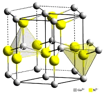
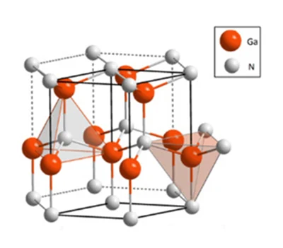
GaN is a compound composed of Gallium (atomic number 31) and Nitrogen (atomic number 7). Gallium is not naturally occurring in elemental form and is typically obtained as a by-product during the smelting of bauxite ore for aluminum production and the processing of sphalerite ore for zinc extraction. GaN wurtzite crystal looks like this:
GaN possesses a robust and stable hexagonal crystal structure, with a high melting point of 4532°F/1700°C, allowing it to operate at significantly elevated temperatures compared to silicon. Additionally, GaN exhibits a much larger band gap than silicon, which signifies the energy required to liberate an electron from its orbit. GaN remains insoluble in water, acid, and alkali at room temperature. Moreover, GaN showcases a high electron mobility transistors of 2000 cm2/Vs, rendering it well-suited for high-frequency applications within the 1 THz range.
The figure of merit serves as a relative measure of the intrinsic, frequency-independent power-handling capability of a material. While GaN possesses slightly lower thermal conductivity than silicon, its higher efficiency permits it to operate at cooler temperatures in silicon-based devices, particularly under high-voltage conditions.
| Difference Between GaN and Silicon | ||
|---|---|---|
| Parameters | GaN | Silicon |
| Wafer Diameter | 3-6 inches | 8 inches |
| Maximum Frequency | 1 THz | 3.8 GHz |
| Maximum Temperature | 600 ̊C | 150 ̊C |
| Peak Electron Velocity | 2.7 x 10⁵m/s | 1 x 10⁵ m/s |
| Band Gap | 1.1 eV | 3.4 eV |
| Electric Field | 3.3 MV/cm | 0.3 MV/cm |
| Power Density | 0.8 W/mm | 7 W/mm |
| Thermal Conductivity | 1.3 W/cmK | 1.5 W/cmK |
| Figure of Merit | 3000 mn*Ec 3 | 1 mn*Ec 3 |
| Johnson Figure of Merit | 27.5 [Ec*vsat]/2p | 1 [Ec*vsat]/2p |
GaN devices offer significant advantages over other semiconductor technologies. They are better than silicon, resulting in reduced energy costs and smaller cooling systems. GaN also provides higher power density, leading to smaller system sizes and reduced component requirements. It enables higher switching frequencies, reducing switching losses and the need for inductive and capacitive components in power circuits. However, GaN devices are more expensive to manufacture than silicon devices. The complex manufacturing process contributes to high dislocation density and challenges in crystal development. GaN’s wide bandgap also makes it difficult to create good metal-semiconductor ohmic contact.
Overall, we can say that Silicon has undoubtedly played a pivotal role in technological advancements, but its potential for further improvement is limited. However, gallium nitride (GaN) emerges as a promising alternative with distinct advantages over silicon.
One area where GaN truly shines is in charging technology. Gallium-based chargers, such as USB C and PD chargers, leverage the superior efficiency and enhanced conductivity of GaN to deliver significantly faster charging capabilities. With GaN devices and accessories, you can expect enhanced performance at competitive costs, thanks to the inherent advantages of gallium nitride over silicon.
By embracing GaN technology, you can unlock a new level of performance in your devices. GaN-based chargers and other GaN-powered accessories offer a promising future for faster, more efficient, and cost-effective charging solutions.
Why are GaN Chargers Better?
GaN fast charges fast and can charge faster than silicon and can handle higher power levels, and, as a result, it’s ideal for uses such as 5G radio and fast-charging accessories. Furthermore, because it is a superior conductor of electricity, it can withstand more power without overheating.
GaN, or Gallium Nitride chargers, exhibit approximately threefold compared to silicon-based chargers in converting power into electricity. Moreover, they boast a significantly smaller and more portable design, enabling them to charge phones roughly ten times faster than standard chargers. This portability ensures their convenience and functionality on the go.
Their resistance to high temperatures contributes to their extended lifespan and reduced heat output. GaN technology, promising enhanced power production with reduced energy consumption, has swiftly gained popularity, particularly in the realm of semiconductor-based chargers.
The prominence of charger gan technology over silicon-based ones lies in their ability to quickly convert electricity into alternating current while consuming less energy. The integration of gan fast charger into smartphones and various electronic devices is an imminent trend. For instance, Samsung Electronics adopted Gan Technology on Chargers for its Galaxy S4 smartphone earlier this year.
Silicon has dominated the realm of transistors since the 1980s, revered for its superior energy absorption and cost-effectiveness in production. However, the rapid evolution of technology has steered the charger landscape towards GaN as a unique and highly conductive material. GaN components facilitate swifter electrical current flow, marking a notable shift in the trajectory of charger development.
Here are why GaN chargers stand out from standard chargers:
- Compact Design:
GaN chargers are a traveler’s dream due to their compact build. Their more efficient semiconductor material allows for a smaller and sleeker design compared to traditional chargers. No more bulky additions in your bag or purse. GaN chargers shine in their portability, making them easy to carry along wherever you go. Their smaller size eliminates bulkiness, whether in your bag or on your desk, offering convenience without taking up much space. - Swift Charging:
For those on the move, GaN chargers are a game-changer. They juice up devices up to three times faster than typical chargers, ensuring your phone gets fully charged in under an hour. No more waiting around for your device to power up! - Enhanced Energy-Saving Solution:
GaN chargers trump traditional ones in energy saving. Their reduced power consumption is eco-friendlier and lighter on your electricity bill. It’s a win-win for both you and the environment. - Cooler and Safer Charging:
One of the significant advantages of GaN chargers is their ability to remain cool and ensure safety during operation. Traditional chargers often generate heat while charging, which can pose safety risks. In contrast, GaN chargers excel in maintaining lower operating temperatures, even when charging devices at high speeds. This characteristic not only enhances user safety but also contributes to the longevity and reliability of the charger itself.
These were all the benefits of GAN chargers, here are some downsides as well. Due to the relatively higher production costs and the limited adoption of GaN technology in mainstream consumer tech products, GaN chargers are currently more expensive to manufacture compared to their silicon-based counterparts. Consequently, the use of GaN technology in chargers by manufacturers is not as widespread as it should be. However, it is anticipated that this situation will improve as production processes become more streamlined and cost-effective.
Despite these challenges, a growing number of businesses are recognizing the remarkable benefits of GaN technology and are beginning to harness its potential. As the advantages of GaN chargers, such as increased energy-saving and smaller form factors, become more widely known, more manufacturers are expected to incorporate GaN technology into their charger offerings. As GaN chargers are still relatively new in the market, their widespread adoption is still in progress. However, reputable retailers like APPHONE offer a reliable source for purchasing GaN chargers.
When it comes to GaN chargers, APPHONE stands out as a brand that offers a great range of high-quality options. Their GaN chargers are known for their exceptional power, making them a top choice for consumers.
What is GaN technology used for?
Since the 1990s, it has been used commonly in light emitting diode leds. Gan or gallium nitride gives off a blue light used for disc-reading in Blu-ray. Additionally, gallium nitride is used in semiconductor power devices, RF components, lasers, and photonics. In the future, we will see GaN in sensor technology.
What is GaN technology in a charger?
A GaN charger is a charger built with gallium nitride rather than the more popular silicon. As a result, it is more compact, energy-saving, and quick to charge than a conventional charger.
Is GaN technology safe?
Yes. Chargers that do not use GaN technology typically get hot while in use, which can be a fire hazard and damaging to your device. GaN chargers stay cool even when they are in use and charging devices at rapid speeds.
What are the benefits of GaN?
The benefits of GaN-based systems include the ability to offer greater efficiency, significantly reduced size and weight, and improved thermal performance.
How is GAN made?
Bulk gallium nitride is a direct band gap semiconductor (band gaps = 3.4 eV) having wurtzite type structure and is the material used for making light-emitting devices that can withstand corrosive environments. Gallium nitride is prepared by the reaction of Ga2O3 with NH3 at elevated temperatures of the order of 1000°C.
Are GaN chargers expensive?
GaN chargers may be more expensive than traditional chargers due to the cost of the gallium nitride semiconductor material.
Do GaN chargers get hot?
No, GaN chargers do not overheat because the use of Gallium Nitride semiconductors allows for higher efficiency and less heat generation compared to traditional chargers using Silicon-based semiconductors.
What are the disadvantages of a GaN charger?
GaN chargers can cost more to make than chargers made with silicon. This is because the production processes for GaN chargers are newer and more specialized. As a result, the charger may have a higher price when sold to customers.
Why is GaN the future?
According to CGD, compared with silicon, GaN-based power electronics can be 20× faster switching/low energy loss and offer up to 3× higher power density and faster charging. In addition, they can be up to 3× smaller and lighter and create a 20% lower system cost.
What is GaN in 5G technology?
GaN is playing a crucial role in the development of 5G technology by enabling faster data transfer speeds and improved efficiency. The wider bandgap of GaN enables it to handle high-frequency signals, making it ideal for use in 5G base stations and other communication infrastructure.
We can say that GaN (Gallium Nitride) technology has emerged as a game-changer in the field of power electronics. Its unique properties and advantages over traditional semiconductor materials, such as silicon, have revolutionized the way we approach power conversion and charging solutions. These advantages translate into tangible benefits for consumers, such as faster charging times, more compact and lightweight chargers, and improved overall performance of electronic devices.
At APPHONE we utilize GaN technology in its charging products. We provide a multi-port 65Gan charger adapter that offers a lightweight and efficient charging experience. Also, we offer a range of plug specifications, including a USB C PD wall charger with a maximum power of 100W and a QC 3.0 USB A car charger with a maximum power of 45W.
APPHONE’s Fast Charger products are designed to provide fast and stable charging for devices in various settings such as home, office, or car. We aim to integrate innovation and customization to deliver superior charging solutions, and offer multi-interface Fast Charger products and customization options to provide a future-grade smart charging experience for devices.
If you are interested in APPHONE’s charging solutions, you can reach out to us to learn more about our products and customization options.
Share This Artcle:

Fast delivery
Fastest delivery within 22 days

Quick proofing
Fastest 3-day proofing cycle

After-sale protection
24-month long warranty

1V1Customer Service
Professional customer service follow-up


